CENAB clean rooms – where the technologies of the future are created
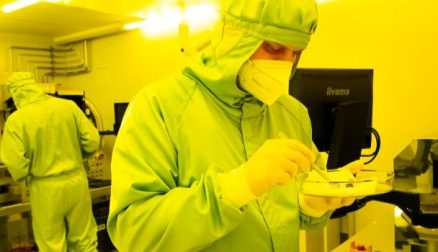
At the Center for Nanomaterials and Biotechnology (CENAB), we are engaged in a wide range of research areas, including work in a clean room laboratory.
This carefully controlled environment minimizes the amount of dust particles, allowing us to prepare micro- and nanoscale structures for advanced sensors, electronics, optical elements, and biomedical applications.
Our starting point is often a silicon wafer, onto which we apply thin photosensitive layers for photolithography using a spin coater. We perform patterning using a photolithographic mask with precise alignment or a direct laser writer – both methods allow the creation of the precise structures necessary for the functionality of the final device.
We use magnetron sputtering to deposit metals and other materials. Quality control is performed on a scanning electron microscope (SEM), which displays details down to nanometers, and on a profilometer, which measures surface roughness and layer thickness.
Clean rooms are just one of the tools we use at CENAB – but without them, many technologies that are now finding their way from the laboratory into practice would not have been developed.
🎥 Watch the video and discover how innovations travel from clean rooms into the world.